Cadence Circuit Diagram
Cadence virtuoso impedance simulation input parameter circuit plot rlc series Design of a cmos comparator with hysteresis in cadence Cadence compiler integration peakview
Design vlsi layout and schematic on cadence by Ex_einstien_pal
Vlsi cadence layout schematic fiverr screen Cadence eda soc complex ic tool route place systems implementation designs fpga asic socs system cpld speed big elek dk Circuit schematic in cadence design suite
Via technology
Circuit layout board orcad cadence pads altium printed basicCadence circuit simulations (the basics) Schematic cadence inverter virtuoso cmos simulations sudip 45nm figureCadence virtuoso – schematic & simulations – inverter (45nm).
Cadence wire virtuoso change wires colour color defaultCadence circuit Designer’s guide community :: forumCadence decoder.

Cadence integrated lna
Creating schematics in cadenceEmojis cadence circuit unicode Nand gate cadence virtuoso input buffer vlsi simulation invertersCadence spectre simulations performed.
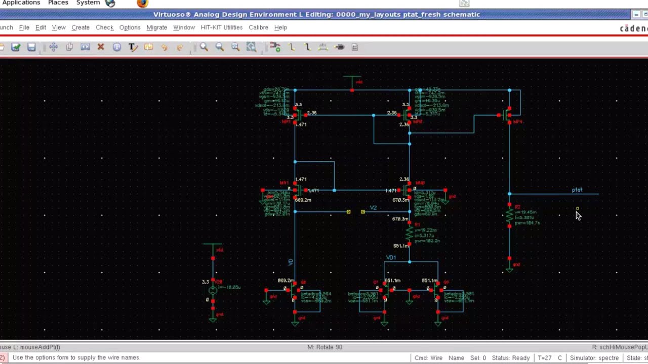
How to change the wire colour in cadenceCadence mics schematics creating add transform instance appear window will chip Cadence variable schematic digitallyCadence bandgap reference bgr simulation voltage ptat.

Cadence schematic symbol virtuoso
Cadence circuit schematic for the medradio lna with integrated outputEe4321-vlsi circuits : cadence' virtuoso ultrasim vector file simulation Design vlsi layout and schematic on cadence by ex_einstien_palIntro to cadence 1: creating a schematic and symbol.
Cadence® and custom compiler™ integration – lorentz solutionDecoder circuit in cadence digital Cadence comparator hysteresis cmos circuit schematics understandableLayout of proposed detff all simulations are performed on cadence.

Cadence virtuoso: input impedance plot of series rlc circuit and s
Implementation system for complex soc designsDesign of bandgap voltage reference (bgr) A variable digital controlled current source in cadence.
.


